It's the time of the year again and we are happy to announce a new release featuring a brand new "Code View" that allows you to program and upload to your microcontroller straight from Fritzing.
To celebrate this, we give you a nice discount on the perfect christmas gift, the Fritzing Creator Kit. Use the discount code FRITZMAS14 to get the kit for 89€ (instead of 95€) and make someone (or yourself) really happy this year. :)
Read more on the release below. This is the new "Code View"! It lets you write your code directly inside Fritzing, and even upload it from there to your microcontroller. It even has a serial monitor. :)
We love this, because it makes it even easier for beginners to get started with interactive electronics. And for more advanced people it's great because you can now keep your code together with the matching circuit--no more confusion!
You can also link to files somewhere else on your hard drive, for example in your local Arduino folder. When the link gets broken, or you just send someone your Fritzing file, don't worry, because there's always a backup stored in the Fritzing fzz file. Right now the upload functionality supports Arduino and PICAXE, but more can be added as long as the platform's IDE has a command line upload option.
The new release also brings with it many new parts, many kindly sponsored by their respective makers. Now you can easily document your circuits and fabricate shields/caps/hats etc. for:
Last but not least, the new release fixes a couple of annoying bugs and generally makes it easier for you to contribute to the code. Setting up your build environment is now just a few easy steps. See the full release notes here.
Download Fritzing 0.9.1b from here, and think about a Fritzmas donation on the way to it.
Happy Fritzmas to everyone!
When we started hacking on Fritzing back in 2007, Google Code was all the hype, and SVN had just replaced CVS as a versioning system. All this has changed for good, and today git (and github) have become the reference for collaborative, open-source development.
We were hesitant until now mostly because of our issue tracker: The one at Google Code has served us wonderfully, and the one at github lacks many of the features that we have come to love (like file attachments and powerful tagging/prioritizing). Also, with the move, original issue reporters will not be notified of changes. Ouch. Luckily, all issues have a backlink to their original Google Code issue, so at least the full history is preserved.
We have also taken the opportunity to move our developer docs over to the github wiki. This way it’s all in one place and you can directly edit it if you have enhancements.
So, we welcome all developers to take a look, watch us, star us, fork us, and most importantly, send us pull requests!
We just noticed that the Linux release did not contain the latest patches, most notably it is missing the Linino boards, an issue with number boxes in languages using comma as decimal separator, and a schematic issue.
The downloads have now been refreshed, so we recommend all Linux users who have already downloaded 0.9 to update. Sorry for this extra step!
We’re happy to announce the release of a new fritzing version! It comes with a bunch of improvements on the inside and outside. Here’s the scoop:
Upgrade to Qt5
Fritzing is written on top the Qt cross-platform application framework. We have upgraded to their latest version Qt5, which brings stability and speed improvements (especially for Mac OS X users). This also enables us to port fritzing to Android, iOS, etc. – that is, in theory. We still need to give that a try. Thanks to Jonathan and contributor Rohan Lloyd!
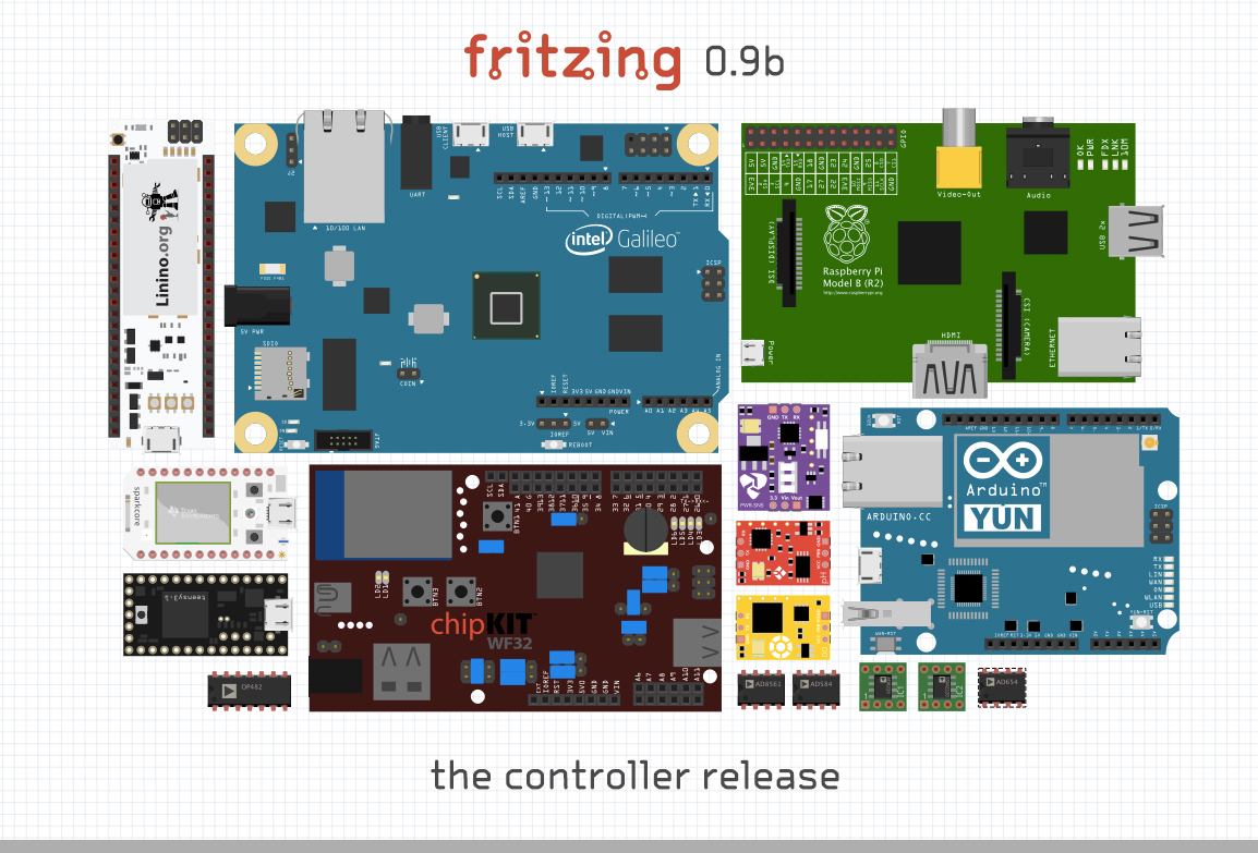
Major part family additions
This release brings a number of new parts, especially a number of popular microcontrollers, as the result of several collaboration efforts:
ADI analog parts, which make use of split schematics and SPICE output, a new feature sponsored by Analog Devices we will write more about soon
several contributed parts, thanks to FrodeLillerud and others
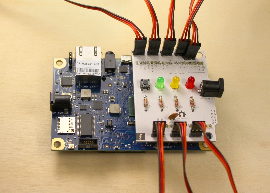
In addition, there are several new PCB shapes for Raspberry Pi, Intel Galileo, SparkCore that will make your boards look cooler. Here’s a snapshot of the Intel Galileo shield in action for the Data Monster: Finally, the usual set of bugfixes, and nicely updated translations: French (thanks to Arnold Dumas!), German (thanks to atalanttore!), Ukrainian (thanks to netavek!).
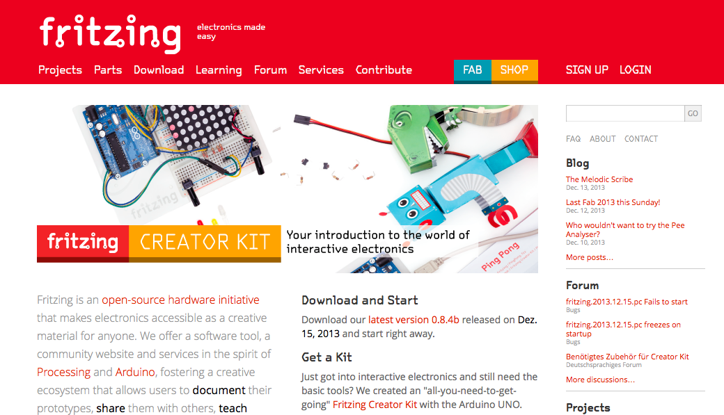
Good news! We have updated the Fritzing website and made it look nice and shiny. And even better: You can now also check out the brand new Fritzing 0.8.5b, released on Dez. 15, 2013.
Fritzing gets a facelift! (special thanks to Christian and Fabian)
new Welcome view
new Fritzing Creator Kit examples (in both English and German)
Tips and Tricks updated
First Time Help now a separate dialog
binaries built using Qt 4.8.5
updated Dutch translation (thanks Dave)
updated German translation
new parts:
Breadboard BB 301 (contributed by Jeremy)
RGB LED WS2812
bug fixes:
Mac OSX Mavericks Parts Bin Hover crash
Saving files with custom parts: sometimes the fzp did not list the latest svg files
Boost 1.54 bug no longer crashes Fritzing
Many part tweaks
This is a high-level summary of changes between each release. If you’re interested in the detailed changes, take a look at the individual code changes.


 Finally, the usual set of bugfixes, and nicely updated translations: French (thanks to Arnold Dumas!), German (thanks to atalanttore!), Ukrainian (thanks to netavek!).